Credit: Cockrell School of Engineering, The University of Texas at Austin.
Faster, smaller, smarter and more energy-efficient chips for everything from consumer electronics to big data to brain-inspired computing could soon be on the way after engineers at The University of Texas at Austin created the smallest memory device yet. And in the process, they figured out the physics dynamic that unlocks dense memory storage capabilities for these tiny devices.
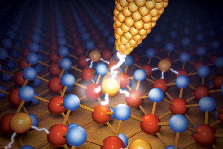
The research published recently in Nature Nanotechnology builds on a discovery from two years ago, when the researchers created what was then the thinnest memory storage device. In this new work, the researchers reduced the size even further, shrinking the cross section area down to just a single square nanometer.
Getting a handle on the physics that pack dense memory storage capability into these devices enabled the ability to make them much smaller. Defects, or holes in the material, provide the key to unlocking the high-density memory storage capability.
“When a single additional metal atom goes into that nanoscale hole and fills it, it confers some of its conductivity into the material, and this leads to a change or memory effect,” said Deji Akinwande, professor in the Department of Electrical and Computer Engineering.
Though they used molybdenum disulfide – also known as MoS2 – as the primary nanomaterial in their study, the researchers think the discovery could apply to hundreds of related atomically thin materials.
The race to make smaller chips and components is all about power and convenience. With smaller processors, you can make more compact computers and phones. But shrinking down chips also decreases their energy demands and increases capacity, which means faster, smarter devices that take less power to operate.
“The results obtained in this work pave the way for developing future generation applications that are of interest to the Department of Defense, such as ultra-dense storage, neuromorphic computing systems, radio-frequency communication systems and more,” said Pani Varanasi, program manager for the U.S. Army Research Office, which funded the research.
The original device – dubbed “atomristor” by the research team – was at the time the thinnest memory storage device ever recorded, with a single atomic layer of thickness. But shrinking a memory device is not just about making it thinner but also building it with a smaller cross-sectional area.
“The scientific holy grail for scaling is going down to a level where a single atom controls the memory function, and this is what we accomplished in the new study,” Akinwande said.
Akinwande’s device falls under the category of memristors, a popular area of memory research, centered around electrical components with the ability to modify resistance between its two terminals without a need for a third terminal in the middle known as the gate. That means they can be smaller than today’s memory devices and boast more storage capacity.
This version of the memristor – developed using the advanced facilities at the Oak Ridge National Laboratory – promises capacity of about 25 terabits per square centimeter. That is 100 times higher memory density per layer compared with commercially available flash memory devices.
###
Media Contact
Nat Levy
[email protected]
Original Source
http://news.
Related Journal Article
http://dx.


