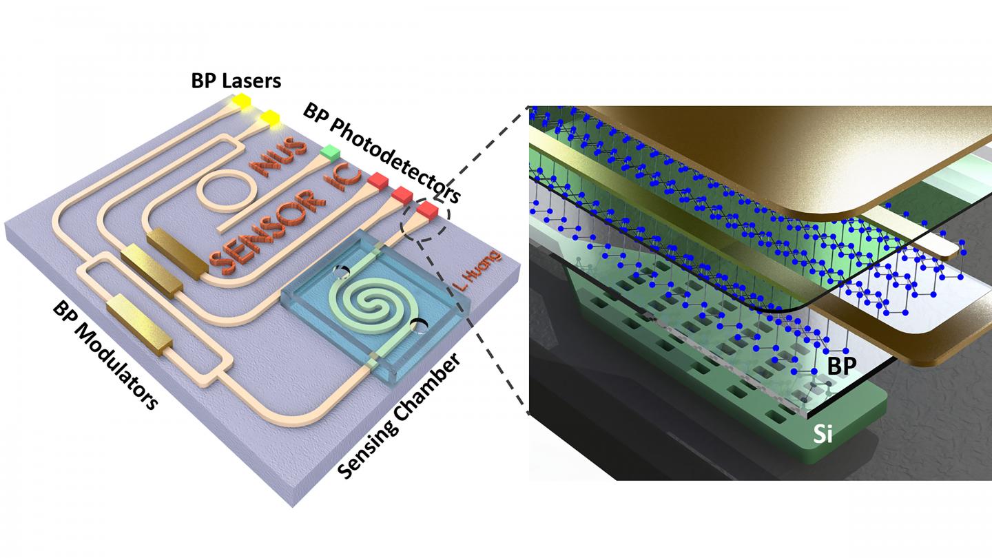
Advances with the versatile material provide a path forward for applications on next-generation optoelectronic chips

Credit: Bowei Dong and Li Huang
WASHINGTON, July 28, 2020 — Many compact systems using mid-infrared technology continue to face compatibility issues when integrating with conventional electronics. Black phosphorus has garnered attention for overcoming these challenges thanks to a wide variety of uses in photonic circuits.
Research published in Applied Physics Reviews, by AIP Publishing, highlights the material’s potential for emerging devices ranging from medical imaging to environment monitoring.
Scientists from the National University of Singapore reviewed the scientific work conducted so far looking into using black phosphorus for next-generation optoelectronics chips. In the paper, the group assesses progress in different components of the chips, from light detection to laser emission.
“Extending the wavelength from near-infrared to mid-infrared enables more diversified functions beyond communication and computing,” said author Kah-Wee Ang. “Sensing is one of the most important potential applications in mid-infrared, as it serves to connect the real world we live in to the virtual system on chip.”
Black phosphorus achieves its promising versatility through the various ways it can be manipulated as a 2D material. These features make it attractive for the field of optoelectronics, in which information conveyed using conventional electron-based chips is combined with emerging technology that uses photons to transmit information.
Going beyond thermal imaging uses, mid-infrared technology may be applied to identifying molecular “fingerprints” or using unique features of the mid-infrared wavelengths to analyze 3D structures and motion to distinguish human-made objects from natural ones.
“If we could realize a compact mid-infrared system, we may be able to actualize applications, such as health monitoring and toxic gas detection, with a small chip in a hand-held device,” Ang said.
By modifying the number of layers, applying a vertical electric field and introducing chemical doping with relative ease, the material can efficiently tune electron energy levels to a device’s desired needs. This precise tuning could be instrumental in the electro-optic modulation that would be required for faster computing and data communication, as well as weak signal detection and spectrum analysis.
Despite its promise, widespread production of atom-thick layers of black phosphorus remains challenging.
“We often rely on exfoliation by tape to obtain thin-film black phosphorus, which is not a fully repeatable process,” Ang said. “Large-scale growth, if achieved, would be a breakthrough to advance black phosphorus-based technology.”
Ang hopes the review helps cement black phosphorus as an essential material in next-generation optoelectronics devices in the coming years and looks to continue working toward high-performance and compact circuit prototypes.
###
The article, “Black phosphorus photonics towards on-chip applications,” is authored by Li Huang and Kah-Wee Ang. The article will appear in Applied Physics Reviews on July 28, 2020 (DOI: 10.1063/5.0005641). After that date, it can be accessed at https:/
ABOUT THE JOURNAL
Applied Physics Reviews features articles on significant and current topics in experimental or theoretical research in applied physics, or in applications of physics to other branches of science and engineering. The journal publishes both original research on pioneering studies of broad interest to the applied physics community, and reviews on established or emerging areas of applied physics. See https:/
Media Contact
Larry Frum
[email protected]
Related Journal Article
http://dx.


