Credit: Argonne National Laboratory
Microelectronics like semiconductor devices are at the heart of the technologies we use each day. As we move into an era where we are stretching the limits of Moore’s Law, it is essential to find new ways to continue to pack more circuitry into each individual device in order to increase the speed and capability of our computers.
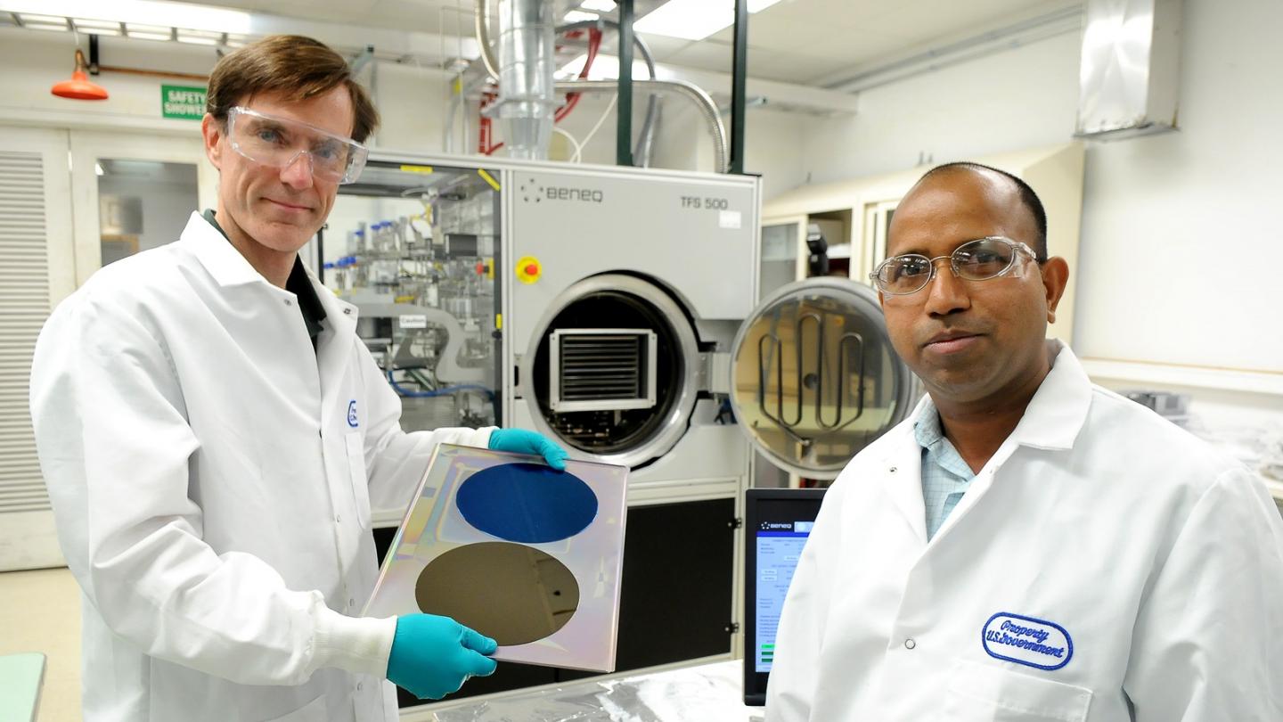
Researchers at the U.S. Department of Energy’s (DOE) Argonne National Laboratory have developed a new technique that could potentially help make these increasingly small but complex devices. The technique, known as molecular layer etching, is detailed in a new paper published in Chemistry of Materials.
“MLE has the potential to help usher in new pathways for fabricating and controlling material geometries at the nanoscale, which could open new doors in microelectronics and extend beyond traditional Moore’s Law scaling.” — Jeff Elam, Argonne chemist
To make microelectronics smaller, manufacturers have to cram in more and more circuitry onto smaller films and 3D structures. Today, this happens by using thin film deposition and etching, techniques to grow or remove films one layer at a time.
“Our ability to control matter at the nanoscale is limited by the kinds of tools we have to add or remove thin layers of material. Molecular layer etching (MLE) is a tool to allow manufacturers and researchers to precisely control the way thin materials, at microscopic and nanoscales, are removed,” said lead author Matthias Young, an assistant professor at the University of Missouri and former postdoctoral researcher at Argonne.
Together with molecular layer deposition (MLD), a deposition technique, MLE can be used to design microscopic architectures. These approaches are analogs of atomic layer deposition (ALD) and atomic layer etching (ALE), the more commonly applied techniques for fabricating microelectronics. However, unlike atomic layering techniques, which deal exclusively with inorganic films, MLD and MLE can be used to grow and remove organic films as well.
How it works
In principle, MLE works by exposing thin films, several nanometers or micrometers thick, to pulses of gas inside a vacuum chamber. The process starts with one gas (Gas A) which, upon entry, reacts with the surface of the film. Next, the film is exposed to a second gas (Gas B). This AB process is repeated until the desired thickness is removed from the film.
“The net effect of A and then B is the removal of a molecular layer from your film,” said Argonne chemist Jeff Elam, a co-author of the study. “If you do that process sequentially, over and over again, you can reduce the thickness of your film to achieve the desired final thickness.”
A key aspect of MLD is that the A and B surface reactions are self-limiting. They only continue until all of the available reactive surface sites are consumed, and then the reactions naturally terminate. This self-limiting behavior is extremely helpful in manufacturing since it is relatively easy to scale the process up to larger substrate sizes.
Researchers tested their approach using alucone, an organic material similar to silicone rubber that has potential applications in flexible electronics. Gas A in their experiment was a lithium-containing salt, and Gas B was trimethyl aluminum (TMA), an organometallic aluminum-based compound.
During the etching process, the lithium compound reacted with the surface of the alucone film in a way that caused the lithium to stick onto the surface and disrupt the chemical bonding in the film. Then, when the TMA was introduced and reacted, it removed the layer of film containing lithium. The lithium serves a sacrificial role — it is deposited on the surface temporarily to break chemical bonds but is then removed by the TMA.
“The process can go on layer by layer like that and you can remove the whole material if you wanted to,” Young said.
Opening new doors in microelectronics
Using this technique can help manufacturers and researchers develop new ways of making nanostructures. The process may also be a safer option for them to use because it is free of halogens, a harsh components of chemicals common in other etching processes. It also has the advantage of being selective; the etching technique can selectively remove MLD layers without affecting nearby ALD layers.
“MLE has the potential to help usher in new pathways for fabricating and controlling material geometries at the nanoscale, which could open new doors in microelectronics and extend beyond traditional Moore’s Law scaling,” Elam said.
###
The paper is titled “Molecular Layer Etching of Metalcone Films Using Lithium Organic Salts and Trimethylaluminum.” Additional co-authors include Angel Yanguas-Gil, Devika Choudhury, Steven Letourneau and Anil Mane.
This research was funded by the Center for Electrochemical Energy Science, an Energy Frontier Research Center supported by DOE’s Office of Science. X-ray reflectivity measurements of the MLD films before and after molecular layer etching were performed at the Argonne Center for Nanoscale Materials, a DOE Office of Science User Facility.
About Argonne’s Center for Nanoscale Materials
The Center for Nanoscale Materials is one of the five DOE Nanoscale Science Research Centers, premier national user facilities for interdisciplinary research at the nanoscale supported by the DOE Office of Science. Together the NSRCs comprise a suite of complementary facilities that provide researchers with state-of-the-art capabilities to fabricate, process, characterize and model nanoscale materials, and constitute the largest infrastructure investment of the National Nanotechnology Initiative. The NSRCs are located at DOE’s Argonne, Brookhaven, Lawrence Berkeley, Oak Ridge, Sandia and Los Alamos National Laboratories. For more information about the DOE NSRCs, please visit https:/
Argonne National Laboratory seeks solutions to pressing national problems in science and technology. The nation’s first national laboratory, Argonne conducts leading-edge basic and applied scientific research in virtually every scientific discipline. Argonne researchers work closely with researchers from hundreds of companies, universities, and federal, state and municipal agencies to help them solve their specific problems, advance America’s scientific leadership and prepare the nation for a better future. With employees from more than 60 nations, Argonne is managed by UChicago Argonne, LLC for the U.S. Department of Energy’s Office of Science.
The U.S. Department of Energy’s Office of Science is the single largest supporter of basic research in the physical sciences in the United States and is working to address some of the most pressing challenges of our time. For more information, visit https:/
Media Contact
Lynn Tefft Hoff
[email protected]
630-252-1750
Original Source
https:/
Related Journal Article
http://dx.


