Silicon-based device may enable variety of photonic applications
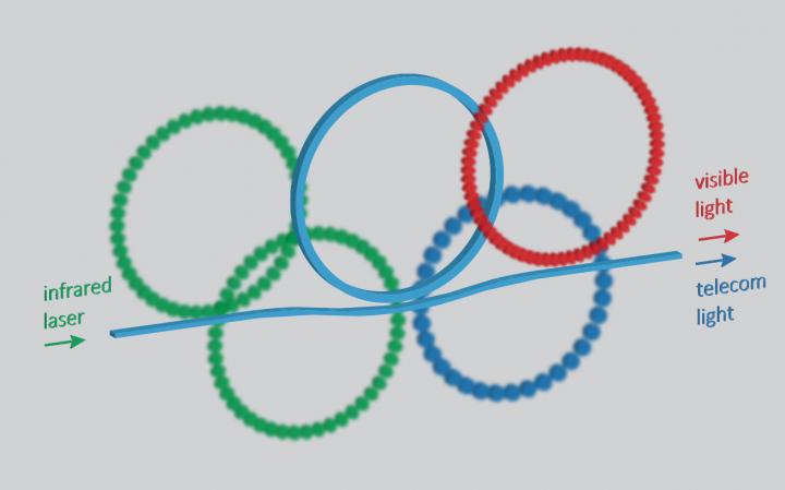
Credit: Xiyuan Lu, NIST/University of Maryland, inspired by the “Olympic rings. “
WASHINGTON — Researchers have designed a new chip-integrated light source that can transform infrared wavelengths into visible wavelengths, which have been difficult to produce with technology based on silicon chips. This flexible approach to on-chip light generation is poised to enable highly miniaturized photonic instrumentation that is easy to manufacture and rugged enough to use outside the lab.
In Optica, The Optical Society’s (OSA) journal for high impact research, investigators from the National Institute of Standards and Technology (NIST), University of Maryland, and University of Colorado describe their new optical parametric oscillator (OPO) light source and show that it can produce output light that is a very different color, or wavelength, than the input light. In addition to creating light at visible wavelengths, the OPO simultaneously generates near-infrared wavelengths that can be used for telecommunication applications.
“Our power-efficient and flexible approach generates coherent laser light across a range of wavelengths wider than what is accessible from direct chip-integrated lasers,” said research team leader Kartik Srinivasan. “The on-chip creation of visible light can be used as part of highly functional compact devices such as chip-based atomic clocks or devices for portable biochemical analyses. Developing the OPO in a silicon photonics platform creates the potential for scalable manufacturing of these devices in commercial fabrication foundries, which could make this approach very cost-effective.”
Exploiting nonlinear processes
Although the response of a material to light typically scales linearly, material properties can change more rapidly in response to light at high power, which creates various nonlinear effects. OPOs are a type of laser that use nonlinear optical effects to create a very broad range of output wavelengths.
The researchers wanted to figure out how to take laser emission at a wavelength readily available with compact chip lasers and combine it with nonlinear nanophotonics to generate laser light at wavelengths that are otherwise hard to reach with silicon photonics platforms.
“Nonlinear optical technologies are already used as integral components of lasers in the world’s best atomic clocks and many laboratory spectroscopy systems,” said Xiyuan Lu, first author of the paper and a NIST-University of Maryland postdoctoral scholar. “Being able to access different types of nonlinear optical functionality, including OPOs, within integrated photonics is important for transitioning technologies currently based in laboratories into platforms that are portable and can be deployed in the field.”
In the new work, the researchers designed an OPO based on a microring made from silicon nitride. This optical component is fed by approximately 1 milliwatt of infrared laser power — about the same amount of power found in a laser pointer. As the light travels around the microring it increases in optical intensity until powerful enough to create a non-linear optical response in silicon nitride. This enables frequency conversion, a nonlinear process that can be used to produce an output wavelength, or frequency, that is different from that of the light going into the system.
“Recent progress in nanophotonic engineering has made this method of frequency conversion very efficient,” said Lu. “A key advance in our work was figuring out how to promote the specific nonlinear interaction of interest while suppressing potential competing nonlinear processes that can arise in this system.”
Testing the light source
The researchers designed the new on-chip light source using detailed electromagnetic simulations. They then made the device and used it to convert 900-nanometer input light to 700-nanometer-wavelength (visible) and 1300-nanometer-wavelength (telecommunications) bands. The OPO accomplished this using less than 2 percent of the pump laser power required by previously reported microresonator OPOs developed for generating widely separated output colors. In the previous cases, both colors generated were in the infrared. With a few simple changes to the microring dimensions, the OPO also produced light in the 780-nm visible and 1500-nanometer telecommunication bands.
The researchers say that the new OPO could be used to make a complete system by combining an inexpensive commercial near-infrared diode laser with an OPO chip that also integrates components such as filters, detectors and a spectroscopy section. They are continuing to look for ways to increase the output power generated from the OPO.
“This work demonstrates that nonlinear nanophotonics is reaching a level of maturity where we can create a design that connects widely separated wavelengths and then achieve enough fabrication control to realize that design, and the predicted performance, in practice,” said Srinivasan. “Going forward, it should be possible to generate a wide range of desired wavelengths using a small number of compact chip lasers combined with flexible and versatile nonlinear nanophotonics.”
###
Paper: X. Lu, G. Moille, A. Singh, Q. Li, D. A. Westly, A. Rao, S.-P. Yu, T. C. Briles, S. B. Papp, K. Srinivasan, “Milliwatt-threshold visible-telecom optical parametric oscillation using silicon nanophotonics,” Optica, 6, 12, 1535-1541 (2019).
DOI: https:/
About Optica
Optica is an open-access, journal dedicated to the rapid dissemination of high-impact peer-reviewed research across the entire spectrum of optics and photonics. Published monthly by The Optical Society (OSA), Optica provides a forum for pioneering research to be swiftly accessed by the international community, whether that research is theoretical or experimental, fundamental or applied. Optica maintains a distinguished editorial board of more than 60 associate editors from around the world and is overseen by Editor-in-Chief Alex Gaeta, Columbia University, USA. For more information, visit Optica.
About The Optical Society
Founded in 1916, The Optical Society (OSA) is the leading professional organization for scientists, engineers, students and business leaders who fuel discoveries, shape real-life applications and accelerate achievements in the science of light. Through world-renowned publications, meetings and membership initiatives, OSA provides quality research, inspired interactions and dedicated resources for its extensive global network of optics and photonics experts. For more information, visit osa.org.
Media Contacts:
Aaron Cohen
(301) 633-6773
[email protected]
[email protected]
Media Contact
James Merrick
[email protected]
202-416-1994
Related Journal Article
http://dx.


