• HOME
  • NEWS
  • EXPLORE
    • CAREER
      • Companies
      • Jobs
    • EVENTS
    • iGEM
      • News
      • Team
    • PHOTOS
    • VIDEO
    • WIKI
  • BLOG
  • COMMUNITY
    • FACEBOOK
    • INSTAGRAM
    • TWITTER
Friday, March 27, 2026
BIOENGINEER.ORG
No Result
View All Result
  • Login
  • HOME
  • NEWS
  • EXPLORE
    • CAREER
      • Companies
      • Jobs
        • Lecturer
        • PhD Studentship
        • Postdoc
        • Research Assistant
    • EVENTS
    • iGEM
      • News
      • Team
    • PHOTOS
    • VIDEO
    • WIKI
  • BLOG
  • COMMUNITY
    • FACEBOOK
    • INSTAGRAM
    • TWITTER
No Result
View All Result
Bioengineer.org
No Result
View All Result
Home NEWS Science News

Metalens grows up

Bioengineer by Bioengineer
December 3, 2019
in Science News
Reading Time: 3 mins read
0
IMAGE
Share on FacebookShare on TwitterShare on LinkedinShare on RedditShare on Telegram

Researchers develop a mass-producible, centimeter-scale metalens for VR, imaging

IMAGE

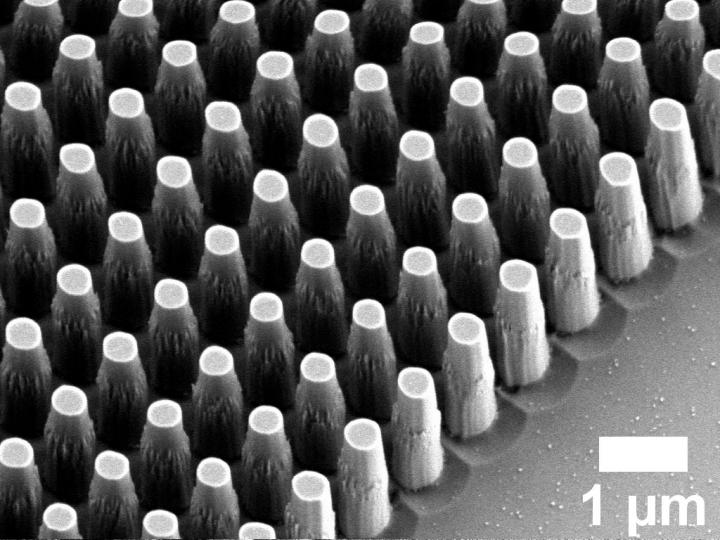
Credit: (Image courtesy of Joon-Suh Park/Harvard SEAS)


Metalenses — flat surfaces that use nanostructures to focus light — are poised to revolutionize everything from microscopy to cameras, sensors, and displays. But so far, most of the lenses have been about the size of a piece of glitter. While lenses this size work well for some applications, a larger lens is needed for low-light conditions, such as an imaging system onboard orbital satellites, and VR applications, where the lens needs to be larger than a pupil.

Now, researchers at the Harvard John A. Paulson School of Engineering and Applied Sciences (SEAS) have developed an all-glass, centimeter-scale metalens in the visible spectrum that can be manufactured using conventional chip fabrication methods.

The research was published in Nano Letters.

“This research paves the way for so-called wafer level cameras for cell phones, where the CMOS chip and the metalenses can be directly stacked on top of each other with easy optical alignment because they are both flat,” said Federico Capasso, the Robert L. Wallace Professor of Applied Physics and Vinton Hayes Senior Research Fellow in Electrical Engineering at SEAS and senior author of the paper. “In the future, the same company can make both the chip and the lenses because both can be made using the same technology: lithography.”

“Previously, we were not able to achieve mass-production of centimeter-scale metalenses at visible wavelengths because we were either using electron-beam lithography, which is too time consuming, or a technique called i-line stepper lithography, which does not have enough resolution to pattern the required subwavelength-sized structures,” said Joon-Suh Park, a Ph.D. candidate at SEAS and first author of the paper.

To mass produce a centimeter-scale metalens, the researchers used a technique called deep-ultraviolet (DUV) projection lithography, which is commonly used to pattern very fine lines and shapes in silicon chips in everything from computers to cell phones. The technique can produce many metalenses per chip, each made of millions of nanoscale elements with a single shot of exposure, like taking a photograph.

The researchers eliminated the time-consuming deposition processes that were required for previous metalenses by etching the nanostructure pattern directly onto a glass surface.

It is the first mass-producible, all-glass, centimeter-scale metalens in the visible spectrum.

While this lens is chromatic, meaning all the different colors of light don’t focus at the same spot, the researchers are working on large-diameter achromatic metalenses.

###

The research was co-authored by Shuyan Zhang, Alan She, Wei Ting Chen, Peng Lin, Kerolos M. A. Yousef, and Ji-Xin Cheng and supported in part by the Defense Advanced Research Projects Agency.

This work was performed in part at the Cornell NanoScale Science & Technology Facility and the Center for Nanoscale Systems at Harvard University, both of which are members of the National Nanotechnology Coordinated Infrastructure (NNCI), which is supported by the National Science Foundation.

Media Contact
Leah Burrows
[email protected]
617-496-1351

Original Source

https://www.seas.harvard.edu/news/2019/12/metalens-grows

Tags: Nanotechnology/MicromachinesOpticsTechnology/Engineering/Computer Science
Share12Tweet8Share2ShareShareShare2

Related Posts

Starburst Winds Drain Supernova Energy Quickly

Starburst Winds Drain Supernova Energy Quickly

March 26, 2026
Decoding the Phosphorus Puzzle: How Microplastics and Hydrochar Transform Nutrient Dynamics in Rice Paddies

Decoding the Phosphorus Puzzle: How Microplastics and Hydrochar Transform Nutrient Dynamics in Rice Paddies

March 26, 2026

Microtubules Found to Actively Ensure Accurate Chromosome Distribution During Cell Division

March 25, 2026

Aversive Learning Hijacks Brain Sugar Sensor

March 25, 2026
Please login to join discussion

POPULAR NEWS

  • blank

    Revolutionary AI Model Enhances Precision in Detecting Food Contamination

    96 shares
    Share 38 Tweet 24
  • Imagine a Social Media Feed That Challenges Your Views Instead of Reinforcing Them

    1003 shares
    Share 397 Tweet 248
  • Uncovering Functions of Cavernous Malformation Proteins in Organoids

    54 shares
    Share 22 Tweet 14
  • Promising Outcomes from First Clinical Trials of Gene Regulation in Epilepsy

    51 shares
    Share 20 Tweet 13

About

We bring you the latest biotechnology news from best research centers and universities around the world. Check our website.

Follow us

Recent News

In-Sensor Cryptography Links Physical Process to Digital Identity

Can Psychosocial Factors Influence Cancer Risk?

Depression Factors in Elderly: Pre vs. Post-COVID Analysis

Subscribe to Blog via Email

Enter your email address to subscribe to this blog and receive notifications of new posts by email.

Join 78 other subscribers
  • Contact Us

Bioengineer.org © Copyright 2023 All Rights Reserved.

Welcome Back!

Login to your account below

Forgotten Password?

Retrieve your password

Please enter your username or email address to reset your password.

Log In
No Result
View All Result
  • Homepages
    • Home Page 1
    • Home Page 2
  • News
  • National
  • Business
  • Health
  • Lifestyle
  • Science

Bioengineer.org © Copyright 2023 All Rights Reserved.