


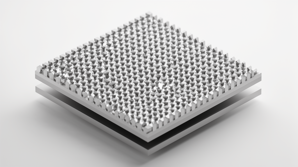
Researchers at the Harvard John A. Paulson School of Engineering and Applied Sciences have engineered an advancement in metasurface design and processing by integrating a built-in, intentionally designed antireflective coating directly into a stacked nanostructure. Described in an experimental study published in Nature Nanotechnology, the advance addresses reflection losses that traditionally degrade the efficiency of ultra-thin optical components. Metasurfaces are flat optical devices patterned with nanoscale structures that precisely control the behavior of light, and they serve as the foundation for compact metalenses currently replacing conventional plastic optics in consumer systems such as smartphone depth sensors.
Led by Federico Capasso, the Robert L. Wallace Professor of Applied Physics and Vinton Hayes Senior Research Fellow in Electrical Engineering, the research team previously established the fabrication of bilayer titanium dioxide metasurfaces composed of two stacked layers of freestanding nanostructures. While these multi-layer architectures offer expanded optical capabilities, reflection at interfaces has remained a persistent physical limitation. Unwanted reflection redirects a fraction of incoming light away from its intended optical path, reducing device transmission and overall operational efficiency.
Under conventional optical manufacturing, mitigating such losses requires applying an external, uniform thin-film antireflection coating across the entire substrate. However, metasurfaces present an inherent geometric obstacle to standard coatings. Although a metasurface may appear uniform to the naked eye, its surface consists of densely arranged nanoscale pillars whose dimensions vary across the device. Because each nanopillar exhibits a different effective refractive index—the physical property quantifying how much light slows down as it travels through a medium—a uniform thin-film coating cannot provide the precise conditions needed to cancel reflections across all local variations simultaneously.
To overcome this limitation, the Harvard researchers co-engineered a dedicated second layer of titanium dioxide with the primary layer to introduce point-by-point antireflection properties across the entire structure. Co-first author and graduate student Davide Cassara, who led the experimental work, noted that the upper nanopillar in the bilayer architecture is tailored specifically to the dimensions and geometry of the pillar beneath it. This structural alignment allows local reflection control, ensuring that antireflective performance is optimized continuously across varying nanostructure geometries.
Beyond curbing parasitic reflections, incorporating a second functional layer introduces substantial degrees of design freedom that single-layer metasurfaces cannot achieve. By altering the geometric shape and spatial orientation of the individual layers, engineers can tailor polarization responses or precisely govern the direction of reflected light. In multi-layer designs, these structural parameters can be configured to support complex optical tasks, including achromatic lenses designed to eliminate chromatic aberrations and produce sharp imaging across broad spectral ranges.
The researchers noted that multi-layer metalens architectures offer functional avenues for emerging technologies such as augmented reality and virtual reality hardware, advanced facial recognition sensors, optical spectroscopy, and biological imaging systems. Furthermore, tailored bilayer nanostructures could potentially function as optical traps for manipulating cold atoms within quantum computing architectures. Cassara also pointed out that the design methodology serves as a general framework that could extend to other optical materials, including silicon, provided compatible bilayer nanofabrication techniques are established.
The study was conducted in collaboration with Corning Incorporated through industry-sponsored research, reflecting an ongoing partnership between academic researchers and industrial materials scientists. Nanofabrication and characterization experiments were performed in part at the Harvard University Center for Nanoscale Systems, a facility within the National Nanotechnology Coordinated Infrastructure supported by the National Science Foundation, alongside research support from the Air Force Office of Scientific Research. Commercialization opportunities and associated intellectual property protections for the bilayer design are being directed through the Harvard Office of Technology Development.
Highlighting the operational significance of the development, Capasso emphasized that antireflection coatings serve as a foundational tool across modern technology to suppress residual reflections that otherwise degrade device performance. According to the research team, applying an integrated coating directly to bilayer metasurfaces represents a first demonstration of its kind, establishing an approach expected to yield wide-ranging consequences across photonics. While single-layer optical metasurfaces have already demonstrated the capacity to manipulate light fields, incorporating the secondary titanium dioxide structure specifically resolves transmission losses without compromising the distinct optical behavior required at different surface positions.
The design also advances practical optical performance by enabling more sophisticated functional configurations, such as achromatic metalenses capable of canceling out color distortion to deliver crisp, clear images. As detailed in the Nature Nanotechnology report, titled ‘Antireflective bilayer metasurfaces with complete wavefront control,’ this local geometric matching prevents the performance trade-offs historically associated with applying blanket thin-film treatments to spatially varying metasurface pillars.
From an industrial perspective, collaborators at Corning Incorporated underscored the importance of coupling optical physics with manufacturing expertise to translate fundamental materials science into commercial devices. Paulo Dainese, a senior principal scientist at Corning, noted that the long-term collaboration between academic researchers and industrial teams combines deep technical competencies to propel optical lens advancements across several sectors. Looking ahead, the researchers anticipate that this bilayer methodology can operate as an adaptable design framework for other optical platforms, potentially encompassing materials such as silicon once compatible multilayer fabrication processes become broadly accessible.
Subject of Research: Bilayer metasurfaces with integrated point-by-point antireflective nanostructures
Article Title: A two-layer metalens for optical devices
Article References: A two-layer metalens for optical devices. Original publication (Bibliographic details unavailable.)
Image Credits: AI Generated
DOI: Not provided
Keywords: metasurfaces, metalenses, antireflective coatings, titanium dioxide, nanophotonics, optics, Federico Capasso, Harvard SEAS, Nature Nanotechnology, refractive index, nanostructures, achromatic lenses, wavefront control, Corning Incorporated, nanofabrication, photonics
News Source: Bethany Barker. (November 20, 2026). Harvard Researchers Develop Bilayer Metasurface With Integrated Antireflective Nanostructures. Scienmag.