

A comprehensive review published in Applied Microscopy details how the combined use of electron diffraction and dark-field transmission electron microscopy (TEM) provides a robust framework for analyzing the structural degrees of freedom in two-dimensional van der Waals materials. These materials possess unique structural characteristics that distinguish them from conventional bulk crystals, primarily due to weak interlayer bonding. This bonding allows for stacking, twisting, and lateral sliding of atomic layers, leading to structural variations such as out-of-plane corrugations and interlayer registry variations. Understanding these variations is essential for linking the physical structure of these materials to their functional properties, including electronic, optical, and ferroic behaviors.
The review emphasizes that transmission electron microscopy offers complementary approaches for this purpose. Electron diffraction provides quantitative crystallographic fingerprints, revealing lattice symmetries, three-dimensional distortions, and strain states with high angular precision. In contrast, dark-field imaging translates selected diffraction information into spatial maps of local structure. When combined, these techniques can resolve complex structural modulations across multiple length scales and under diverse experimental conditions. This integration makes TEM uniquely capable of resolving the complex structural landscape of 2D materials, capturing subtle structural modulations that are otherwise difficult to detect.
Large-area orientation and grain boundary analysis is a critical application of these methods, particularly for materials grown by scalable techniques such as chemical vapor deposition. In such samples, rotational disorder and grain boundaries introduce variations in carrier mobility, strain accumulation, and interfacial reactivity. Dark-field TEM meets the need for large-area orientation mapping through Bragg spot-filtered imaging. By isolating specific diffraction vectors, researchers can construct complete orientation maps that visualize grain orientation, misorientation angles, and boundary distributions with sub-micrometer spatial resolution. This approach has been particularly powerful in monolayer and few-layer graphene, where chemical vapor deposition growth often results in a patchwork of rotational grains.
Specific studies have demonstrated the utility of these techniques in identifying grain boundaries composed of periodic pentagon-heptagon dislocation cores in monolayer graphene. In related work, researchers used dark-field TEM to locate and resolve grain boundaries in polycrystalline graphene before fabricating Hall bar devices intersecting these boundaries. Electrical transport across boundaries with known structures showed that well-connected, atomically sharp boundaries had only slightly reduced conductance compared to single grains. Conversely, poorly stitched boundaries containing amorphous or overlapping regions could be up to an order of magnitude more resistive. These results highlight how dark-field TEM, when combined with complementary high-resolution imaging, can directly connect grain boundary structures to the optical and electronic responses of 2D semiconductors.
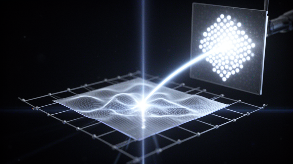
The review also addresses the quantification of three-dimensional structural modulation, noting that 2D materials can exhibit significant out-of-plane distortions caused by thermal fluctuations or strain relaxation. These corrugations are closely linked to the fundamental stability and functionality of the material, influencing electron-phonon coupling and modulating the band structure. Electron diffraction provides a sensitive and non-destructive means to probe these corrugations through analysis of the shape and broadening of Bragg reflections. For a perfectly flat 2D crystal, the reciprocal lattice consists of elongated rods that intersect the Ewald sphere as sharp Bragg spots. However, a corrugated membrane has a distribution of local surface normals, which modifies the reciprocal lattice from straight rods to cone-like shapes.
Tilt-series diffraction experiments on suspended monolayer graphene have shown cone-like broadening with cone angles of approximately 8 to 11 degrees, corresponding to surface-normal variations of about 5 to 6 degrees. In bilayer graphene, the variation in surface normal was found to be 2 degrees, presumably due to the increase in membrane stiffness. While analogous tilt-series diffraction broadening analyses are well established for graphene, extending the same protocol to other 2D materials such as hexagonal boron nitride and transition metal dichalcogenides remains an opportunity. Systematic, diffraction-based comparisons across layer numbers, substrates, and processing conditions would help quantify how process history shapes the final morphology of these materials.
Layer number identification is another key area where these techniques are applied. The number of atomic layers in 2D materials critically influences their electronic and optical properties. For example, transition metal dichalcogenides exhibit a thickness-dependent transition from a direct to an indirect bandgap. In TEM, the layer number can be determined without atomic-resolution imaging by exploiting the sensitivity of specific diffraction intensities to the number of scattering planes. In graphene, the second-order Bragg peaks exhibit an intensity that scales approximately with the square of the number of layers under kinematic conditions. This strong thickness dependence enables robust layer-number identification in dark-field TEM images, allowing monolayer, bilayer, and few-layer regions to be discriminated over large fields of view.
Stacking order identification and domain boundary mapping are also discussed in the review. In bilayer graphene, the most commonly studied stacking orders are Bernal and its mirror-symmetric counterpart. Although these differ only by an in-plane translation, they can exhibit contrasting dark-field TEM intensities due to phase interference between electron waves diffracted from the two layers. Tilting the sample away from the zone axis modifies the phase term in the bilayer’s structure-factor such that one stacking moves toward more constructive interference while the other moves toward more destructive interference. This principle established that different stacking domains can be unambiguously mapped over large areas with nanometer-scale resolution. The same tilt-assisted approach has been applied to other layered crystals with lower symmetries, including hexagonal boron nitride and transition metal dichalcogenides.
In twisted 2D materials, dark-field TEM is a powerful tool for probing the reconstructed patterns that emerge from lattice relaxation. In small-angle twisted bilayer graphene, relaxation produces triangular domains separated by soliton-like boundaries that form an interconnected triangular network. These boundaries can be directly visualized using second-order Bragg reflections, where their visibility depends on the relationship between the reciprocal lattice vector and the Burgers vector describing the stacking change across the boundary. Imaging with multiple inequivalent second-order reflections allows for the identification of which boundary sets vanish in each image, enabling assignment of the Burgers vector to each family and quantitative mapping of the dislocation network.
The review further explores revealing lattice symmetry through Friedel pair breaking. In monolayer transition metal dichalcogenides with trigonal prismatic coordination, the absence of an in-plane inversion center gives rise to a well-defined crystallographic polarity. This polarity underpins valley-contrasting optical selection rules and layer-dependent ferroelectric phenomena. In electron diffraction, polarity can be probed by comparing the intensities of a Friedel pair of reflections. Recent analysis and experiment have shown that even an atomically thin polar crystal can break Friedel symmetry when its in-plane inversion symmetry is absent. These effects lead to polarity-dependent intensity asymmetry between conjugate reflections, regardless of the incident beam energy. By selecting an appropriate Bragg reflection sensitive to polarity and forming a dark-field TEM image, polar domains can be directly visualized over large areas.
In-situ and operando transmission electron microscopy offer a unique way to monitor the structural processes occurring in 2D materials under external stimuli. These techniques can distinguish structural variants such as different crystal phases, charge-density-wave modulations, or stacking domains, all of which directly influence the functional properties of the material. In twisted hexagonal boron nitride and transition metal dichalcogenides, unconventional forms of ferroelectric behavior have recently been reported. Researchers addressed the structural origins of these responses by fabricating a double-capacitor device geometry and performing operando dark-field TEM imaging to follow, in real time, the reconfiguration of polar domains during electrical switching. Their measurements revealed that distinct modes of domain evolution correlate with either ferroelectric-like or antiferroelectric-like responses.
Another example involves the study of the structural evolution of few-layer molybdenum telluride during its anisotropic layer-by-layer phase transition. By combining diffraction and dark-field imaging, researchers were able to resolve the spatial progression of the transition front with high spatial and temporal resolution. This revealed that the phase transformation proceeds through a sequence of discrete layer conversions rather than a uniform transformation. This insight clarified the microscopic pathway of a technologically important phase change relevant to phase-change memory and reconfigurable electronics. Similarly, other studies have combined dark-field TEM with time-resolved electron diffraction to investigate how charge-density-wave order responds to applied electrical pulses, showing that defects play a decisive role in mediating the recovery pathway.
Looking ahead, the review suggests that integrating four-dimensional scanning transmission electron microscopy into in-situ and operando workflows will provide multi-channel structural information from a single dataset. This includes strain, symmetry breaking, and phase coexistence, greatly enhancing the efficiency of dynamic experiments. Coupling these high-dimensional datasets with machine learning will further accelerate analysis, enabling rapid, automated, and more sensitive detection of subtle structural changes. Together, these developments will expand the scope of diffraction and dark-field TEM from static structural mapping to real-time, multi-parameter tracking of structure-function relationships in 2D materials under realistic operating conditions.
Subject of Research: Structural analysis of 2D van der Waals materials using electron diffraction and dark-field TEM
Article Title: Electron diffraction and dark-field TEM for structural analysis of 2D van der Waals materials
Article References: Kim, B., Park, D., Jeong, S., & Yoo, H. (2025). Electron diffraction and dark-field TEM for structural analysis of 2D van der Waals materials. Applied Microscopy, 55(1), Article 11. https://doi.org/10.1186/s42649-025-00117-3
Image Credits: AI Generated
DOI: 10.1186/s42649-025-00117-3
Keywords: 2D materials, van der Waals, electron diffraction, dark-field TEM, structural analysis, grain boundaries, stacking order, in-situ TEM, Applied Microscopy, materials science, Electron, diffraction
News Source: Denise Maddox. (November 8, 2026). Electron Diffraction Maps Structural Dynamics in 2D Materials. Scienmag.