


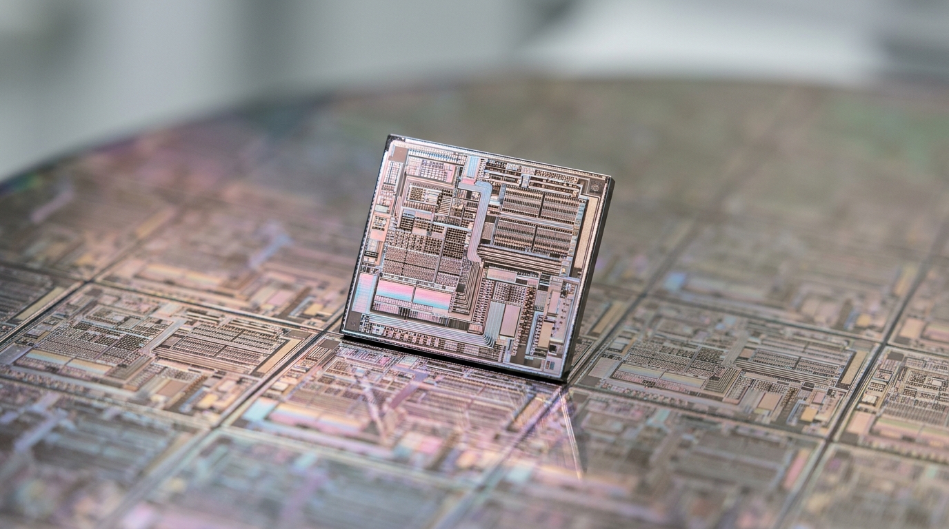
Two major U.S. Department of Energy national laboratories and NY Creates have launched a pilot program funded by the DOE Office of Science to accelerate the development of advanced semiconductor chips. The initiative was formally announced in September during a kickoff meeting held at the Albany NanoTech Complex in Albany, New York, which is owned and operated by the nonprofit New York Center for Research, Economic Advancement, Technology, Engineering, and Science. The collaborative program is structured to facilitate direct access to world-class scientific User Facilities and institutional expertise at Brookhaven National Laboratory and Lawrence Berkeley National Laboratory for commercial chip manufacturers. By establishing these pathways, the initiative seeks to foster active connections between national laboratory scientists and industrial partners who transform scientific advances into commercial microelectronics products.
Under the framework of the pilot program, participating microelectronics companies will work directly with national laboratory experts to design dedicated experiments targeting the most pressing challenges identified across the semiconductor industry. The program is designed to lower operational and structural barriers that previously hindered private industrial partners from utilizing the specialized, state-of-the-art instruments housed at national laboratory complexes. Program organizers emphasize that streamlining this access will accelerate the deployment of laboratory discoveries and manufacturing innovations into the next generation of semiconductor chips, providing essential hardware foundations for computational technologies including advanced applications in Super Intelligence.
Bindu Nair, the DOE Associate Director of Science for Basic Energy Sciences, stated that the pilot program will explore new avenues for bolstering United States technological leadership across the semiconductor manufacturing sector. Nair emphasized that by strategically leveraging the distinct capabilities and scientific expertise present at each participating facility, the collaboration can significantly enhance national competitiveness in a domain that remains of paramount importance to both strategic and economic security. Through a recurring schedule of technical exchanges and collaborative workshops, the partner institutions plan to translate industrial microelectronics challenges into concrete approaches for semiconductor patterning and advanced materials characterization.
The collaborative efforts under the pilot program will focus primarily on two foundational areas of semiconductor hardware development: lithography and metrology. In chip fabrication, lithography serves as the critical patterning process used to transfer microscale electronic circuits onto silicon wafers, while metrology provides the high-precision measurement, imaging, and characterization required to evaluate the physical, structural, and chemical properties of semiconductor materials. The initiative aims to coordinate high-priority research agendas, execute targeted experimental runs, and accelerate data analysis workflows to advance both disciplines in tandem with industrial production needs.
Extreme ultraviolet, or EUV, lithography utilizes short-wavelength ultraviolet light to etch exceptionally fine and precise circuitry patterns onto silicon wafers, serving as the foundational manufacturing technology for leading-edge, high-performance microelectronics. This advanced lithographic process is vital for producing the small, fast, and energy-efficient chips required to meet escalating computational demands across intensive data applications. By extending circuit miniaturization, EUV lithography improves operating performance while reducing overall power consumption, which is critical for meeting broader computing energy requirements and strengthening domestic semiconductor manufacturing. Furthermore, the integration of high numerical aperture, or High NA, EUV technology substantially increases lithographic resolution, permitting the creation of even smaller and more power-efficient devices.
To support these technological requirements, the DOE User Facilities located at Lawrence Berkeley National Laboratory offer specialized equipment dedicated to advanced patterning and materials analysis. Berkeley Lab houses capabilities for high numerical aperture extreme ultraviolet patterning alongside nanoscale materials characterization within the Advanced Light Source and the Molecular Foundry. Furthermore, Berkeley Lab contributes extensive scientific computing models, chemical and materials science expertise, soft X-ray synchrotron tools, and specialized EUV infrastructure developed over decades of research conducted at its Center for X-ray Optics.
Complementing the capabilities at Berkeley Lab, Brookhaven National Laboratory provides advanced synchrotron and nanomaterials facilities to address complex semiconductor metrology and imaging requirements. Brookhaven operates the National Synchrotron Light Source II and the Center for Functional Nanomaterials, offering synchrotron-based X-ray metrology, nanoscale imaging, spectroscopy, scattering, and materials characterization. These analytical tools allow industrial and academic researchers to rapidly screen, test, and evaluate novel candidate materials and processing techniques required for next-generation EUV lithography platforms.
NY Creates serves as a vital co-development and execution partner in the initiative, providing a practical bridge between laboratory research and commercial fabrication facilities. Operating out of Albany, New York, the organization manages an advanced semiconductor research and development hub that currently features low numerical aperture EUV systems and is expanding to include high numerical aperture EUV tools at its High NA EUV Lithography Center. NY Creates will contribute semiconductor manufacturing perspectives, translate industrial processing and materials challenges into joint research opportunities, and actively engage industry super-users to validate, refine, and accelerate emerging technologies toward full commercial adoption.
Leadership across the participating institutions emphasized the strategic alignment of the joint initiative. Dave Anderson, president and chief executive officer of NY Creates, noted that combining DOE laboratory capabilities with NY Creates’ industrial ecosystem and High NA EUV Lithography Center creates a unique domestic environment for developing next-generation microelectronics and building a robust domestic production base. Brookhaven National Laboratory Director John Hill highlighted Brookhaven’s established relationship with NY Creates, noting that previous collaborations leveraged high-resolution X-ray beamlines at NSLS-II to conduct specialized studies for cutting-edge semiconductor technologies to accelerate domestic leadership in microelectronics.
Jeff Neaton, Interim Deputy Laboratory Director for Research and Chief Research Officer at Berkeley Lab, noted that the technical challenges presented by next-generation EUV lithography necessitate breakthroughs in nanoscale patterning science, advanced fabrication equipment, characterization tools, and computational modeling. Supported by the DOE Office of Science—the nation’s largest supporter of basic research in the physical sciences—the pilot program is structured to broaden awareness of national user facilities, establish structured analysis workflows, and address pre-competitive technical challenges alongside semiconductor manufacturers, tool builders, and materials developers.
Beyond its facility hosting duties in Albany, NY Creates operates as an established lab-to-fab bridge designed to foster public-private and industry-academic partnerships for technology development and innovation. The organization attracts and leads industry-connected innovation and commercialization projects that secure significant investment, advance research and development in emerging technologies, and generate the jobs of tomorrow. Across its operations, NY Creates runs some of the most advanced facilities in the world, boasting more than 2,700 industry experts and faculty. Furthermore, the organization manages combined public and private investments totaling $25 billion, placing it at the global epicenter of high-tech innovation and commercialization. Demonstrating the close institutional alignment among the project partners, representatives from Brookhaven National Laboratory, Lawrence Berkeley National Laboratory, and the U.S. Department of Energy Office of Science recently visited NY Creates to engage with the facility.
The institutional foundation provided by Brookhaven National Laboratory adds critical experimental breadth to the microelectronics partnership. As one of ten national laboratories overseen and primarily funded by the U.S. Department of Energy Office of Science, Brookhaven conducts research across the physical, biological, and environmental sciences, as well as in energy technologies, computation, quantum technologies, and national security. In addition to conducting internal scientific investigations, Brookhaven builds and operates major scientific facilities that are made available to university, industry, and government researchers. The laboratory is operated and managed by Brookhaven Science Associates, an organizational partnership founded by Stony Brook University and Battelle. Within this operational framework, Stony Brook University represents the single largest academic user of Brookhaven’s laboratory facilities, while Battelle contributes its institutional capacity as a nonprofit applied science and technology organization.
Lawrence Berkeley National Laboratory brings a complementary institutional history and broad multidisciplinary scope to the collaborative effort. Managed by the University of California for the U.S. Department of Energy Office of Science, Berkeley Lab operates as a multiprogram national laboratory committed to groundbreaking research focused on discovery science and solutions for abundant and reliable energy supplies. Founded in 1931 on the foundational belief that the biggest problems are best addressed by teams, Berkeley Lab and its scientists have been recognized with 16 Nobel Prizes. The laboratory’s research expertise spans materials, chemistry, physics, biology, earth and environmental science, mathematics, and computing. Scientific investigators from around the world rely on Berkeley Lab’s world-class facilities for their own pioneering research, providing an experienced research infrastructure to support advanced materials characterization and nanoscale science.
By connecting laboratory capabilities with industrial manufacturing perspective, the pilot program directly targets the scientific challenges associated with pushing the boundaries of Moore’s Law with extreme ultraviolet lithography. The collaborative initiative helps translate the operational challenges that the semiconductor industry currently faces, in terms of both the materials used and the processes for manufacturing, into concrete opportunities for joint exploration and technological development. Utilizing the state-of-the-art instruments at the national user facilities, researchers can rapidly screen and evaluate new materials and techniques needed for EUV lithography platforms. Program leaders emphasize that addressing these foundational manufacturing and metrology challenges will support the development of next-generation EUV lithography capabilities as well as a domestic production base for novel microelectronics devices. Through targeted collaborative experiments and sustained technical exchanges, this inter-institutional effort establishes a practical bridge to transition basic laboratory discoveries into scalable innovations that reinforce United States technological leadership across the semiconductor industry.
Subject of Research: Semiconductor manufacturing and extreme ultraviolet lithography research
Article Title: DOE labs and NY Creates partner to advance US microelectronics
Article References: DOE labs and NY Creates partner to advance US microelectronics. Original publication (Bibliographic details unavailable.)
Image Credits: AI Generated
DOI: Not provided
Keywords: semiconductors, microelectronics, extreme ultraviolet lithography, materials characterization, Department of Energy, Brookhaven National Laboratory, Lawrence Berkeley National Laboratory, NY Creates, labs, Creates, partner, advance
News Source: Denise Maddox. (November 8, 2026). DOE Labs and NY Creates Launch Initiative for Next-Generation Semiconductor Chips. Scienmag.